Product Categories
Accurate and informative data are the key to research discovery and routine testing. At SiMPore we strive to develop sample preparation substrates and membrane filtration products that enable superior data capture and analysis. Our substrates are tailored to provide unmatched performance for a variety of applications.
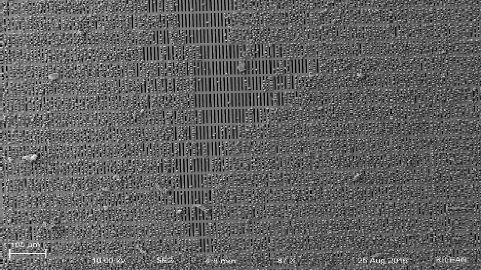
Range of porous or non-porous materials, thicknesses, and thin-film coatings available.

Ideal substrates for X-Ray microscopy and spectroscopy, compatible with a range of vacuum and temperature conditions.
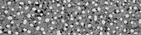
Save time and avoid lengthy error-prone transfers by capturing and then analyzing microplastics on the same substrate with optical, infrared, or Raman microscopy.
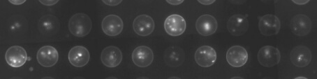
Culture unique single-cell spheroids with MicroBubble Arrays.
Analyze barrier cell models with exceptional resolution with µSiM-CV.
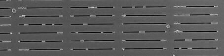
Nanomembrane-enabled nanoparticle isolation and analysis.
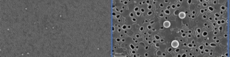
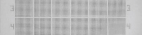
Nanoporous, microporous, and microslit membrane chips, available in a number of cut-off sizes
Advanced Technology
We use proprietary etching methods and the latest in MEMS and thin-film processing to fabricate freely suspended silicon membranes.
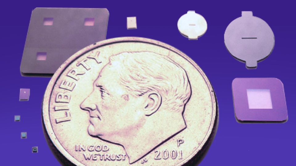
Custom Fabrication
No matter your membrane application, we’ll ensure the perfect product to meet your unique needs.